Thin Films and Flexible Electronics
05 May 2020
Devrim Özaydın
Tags :
Products based on thin films and flexible printed electronics, which are expected to make their way into our homes in the near future, are shown in Figure 1.
As can be seen, a large-screen TV is mounted on the wall. It is lightweight, thin and flexible. The TV panel itself consists of an OLED (organic light emitting diode), with an active matrix back plane composed of organic transistors and metallic nano ink circuits. The person sitting at the table is reading a newspaper, but it is no ordinary newspaper. It is actually a foldable display sheet. The wall behind the TV, with its patterned design, is not simply a wall covered with patterned wallpaper but is actually a DSSC (dye sensitized solar cell) wall that recycles electrical energy from the lighting inside the house. The gadgets on the table –a smartphone, playing cards and notebook PC– are not merely lying there but are being wirelessly charged via the communication sheet on the table. The robot walking in the room possesses soft and flexible skin with plenty of flexible sensors, to prevent it from injuring people or pets or damaging furniture. The floor also has a sensor network beneath the carpet that senses any movement above the floor. The sensor network also needs to be soft. The curtain is not a straightforward piece of cotton fabric. Its outside face is an organic thin film type of solar cell, while its inside face is an OLED lighting panel. The solar cell provides electricity for the internal lighting, and the curtain itself works as a standalone flexible device. On the roof there is, of course, a solar cell module, possibly formed from inorganic thin film. Close inspection of the person sitting at the table reveals that he has some sort of device on his shoulder: a health monitor seal on his shirt. The seal monitors his temperature, blood pressure, pulse, sugar level and other important health parameters and sensors transmit health data to his doctor via a cell phone.
All in all, a variety of flexible and printed electronics products will be a regular feature of our lives in the near future and will add extra ease and comfort to our daily routines. These devices will not be noticeable to people because they will be so thin and lightweight, and they will match the contours of walls, clothes and even skin; they will certainly be energy- eficient and, above all, aGordable. [1] In other words, thin films and flexible electronics are on their way…
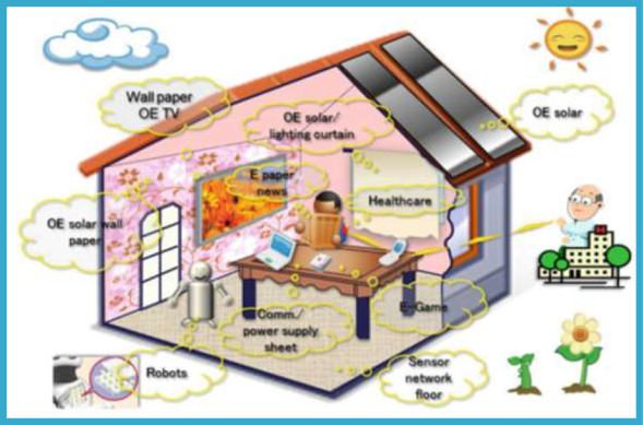
Figure 1: Thin Films and Flexible Electronics in the near future1
Kordsa’s new R&D Platform: Thin Films and Flexible Electronics
After completing several detailed workshops, in March 2019 Kordsa launched a new R&D platform “Thin Films and Flexible Electronics” in partnership with Sabancı University.
Step by step, Kordsa and Sabanci University Platform members started to understand and develop thin films and flexible electronics technology in line with an open innovation concept. The Platform is now in contact with some universities, institutions and companies in Turkey, the US and Europe, with the aim of developing this new technology and creating potential new business.
The team engaged straight away with a new project in May 2019, Nano- sis- 1004, funded by the leading Turkish research body, TUBITAK. Kordsa is coordinating the project, and its current partners are İstanbul Technical University, Sabancı University, Yeditepe University, TUBI- TAK and Arçelik. An additional European institute is due to join. The aim of the project is to develop a new generation of flexible-type wearable healthcare sensors.
Other new projects are expected to emerge, once Kordsa has purchased new lab and pilot machines suitable for flexible electronics technology.
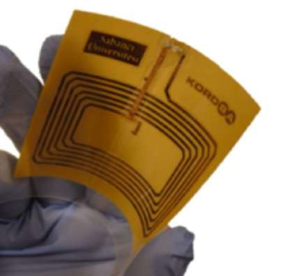
Figure 2: The first flexible sensor prototype developed by Sabanci Univer- sity and Kordsa in April 2019.
Before we go on to consider more details, the reader may be asking this basic question:
- What are thin film and flexible electronics? A thin film is a layer of material ranging in thickness from fractions of a nanometer to several micrometers.
Flexible electronics are devices built using conformable or stretchable substrates, generally plastic but also metal foil, paper and flexible glass.
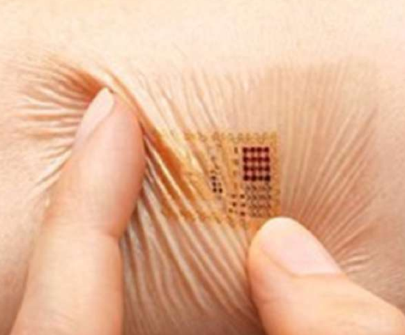
Figure 3: A sample of thin film
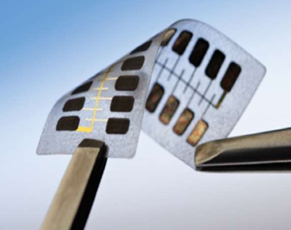
Figure 4: A sample of flexible electronics
Thin Films
Thanks to the advances in nanotechnology, thin films and thin film devices have been developed for a vast range of conventional and emerging applications. This has been greatly helped by progress in producing conducting polymers, molecular semiconductors and carbon nanotubes, by exploiting graphene as a raw material, making use of techniques for obtaining high surface area, controlling nanostructure for eGective charge transfer and exploiting unique physical and chemi- cal features [2].
The diGerence between a thin and a thick film is defined rather vaguely in the literature; usually 1 µm (1000 nm) of thickness is said to be the border between thin and thick films. Another approach is to define the type of film according to its surface or bulk-like properties. For instance, surfaces that require to be more than one micrometer thick can still be classified as thin films [3].
With semiconductors, it is vital that some quantity of functional materi- al (organic molecules, polymers, metals, metal oxides or dielectrics) is deposited on very thin films. This is due to the fact that the semiconduc- tor sector has been witnessing constant miniaturization since the 1950s. When the first transistor was made, it was only good for a single use. Today, however, millions of transistors can fit on a small chip capable of running multiple functions, as is particularly evident with cell phones.
When we talk about thin films, the thicknesses of such electronically active films range from a few nanometers –coating just a few atoms with a few more– to a few microns. As such, thin films possess diGerent structural, optical and electrical properties compared to their bulk form. For example, graphite is a bulk form made up of millions of carbon atoms, which gives it its black color and thus renders it non-transparent; in contrast, graphene is transparent when deposited in one atomic layer. When deposited in very thin layers, atoms can be aligned perfectly in three dimensions without the defects demonstrated by their bulk counterparts. This actually enables magnificent electrical conductivities and the charge carrier mobilities required for electronic applications. Another advantage of thin films is that very low resistivity can be obtained by the meticulous alignment of atoms in them. This allows new electronic devices to run on very small voltages, as in the case of electro- chromic, light-emitting diodes or sensors.
Coating flexible substrates with very thin layers of functional materials makes it possible for people to produce devices that could not have been made before, such as electronic skin, flexible displays and flexible solar cells. As the amount of functional material is decreased, it can nonethe- less adjust well to the substrate, thereby avoiding mechanical brittle- ness. For this purpose, the deposition methods used have high through- put but are also very precise. Among the technologies deployed to create thin films are vacuum-coating technologies (using chemical vapor or physical vapor deposition) and solution process-based (roll-to-roll) coating.
Flexible Electronics
The term “Flexible electronics”, usually called printed electronics, refers to functional electronics fabricated by laying conductive lines using one of several printing methods. The origin of this technology was to replace conventional silicon electronics with lower cost devices. But there are more benefits now. Companies are now focusing on a wide range of technologies including sensors, smart textiles and flexible displays with the goal of complementing silicon electronics and, in many cases, yielding high value or unique features.
Flexible electronics essentially consist of two layers –substrate and functional materials (eg. conductive inks, dielectrics, etc.). In recent years, plastics (particularly polyimide and polyester) have been the substance of choice in the substrate segment.
Why are flexible electronics preferred?
There are several advantages of flexible electronics compared to conventional silicon electronics. The key advantages of thin films and flexible electronics are as follows:
- Flexibility - stretchability
- Disposability and sustainability
- Increased potential for digitalization
- Light weight
- Low cost processing
- Miniaturization, small and eficient systems
- Scalability, modularity and easier reconfiguration
Flexible electronics technology can be found in the market but is relatively rare. However, there is a huge potential market that will require much time and eGort to develop. Major market products are as follows:
- Lighting (OLED)
- Organic and inorganic photovoltaics, solar cells
- Displays
- Integrated smart systems (RFID, sports and healthcare devices, smart cards and smart textiles)
- Electronics and components (memories, antennas, batteries, wiring and interconnects and other components)
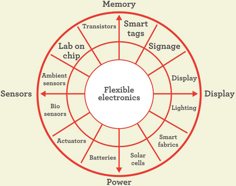
Figure 5: Categories of flexible electronics products
The flexible and printed electronics market is at a relatively early stage of its developm ent. For many years, traditional rigid, fabricated electron- ic modules dominated the market, after which advancem ents in 3D printing started to drive the market. Growth in the last decade has been very quick, ranging from USD 3.8 billion in 2009 to USD 31.6 billion in 2018. [4]
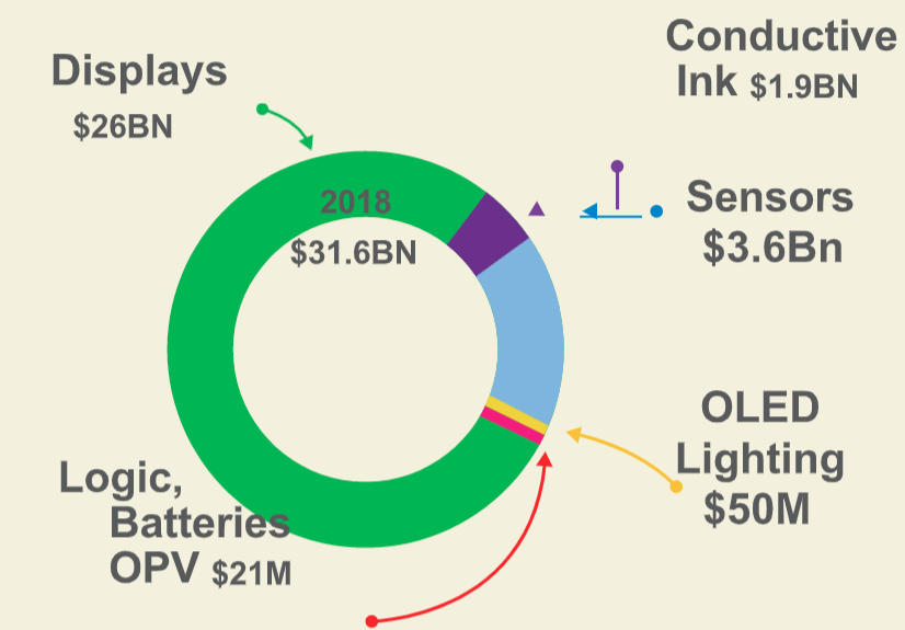
Figure 6: The current flexible electronic market [4]
Technologies for flexible electronics will be major diGerentiators in the next generation of consumer and computing devices. Some of these devices are expected to be among the fastest growing product catego- ries over the next decade.
Flexible printed electronics can be manufactured using a variety of technologies, which can be categorized into two main groups: Non-Con- tact and Contact Printing.
Roll-to-Roll Printing is the most convenient, simplest and cheapest printing technology available on the market.
We will discuss these technologies in the following issue of Reinforcer Magazine.
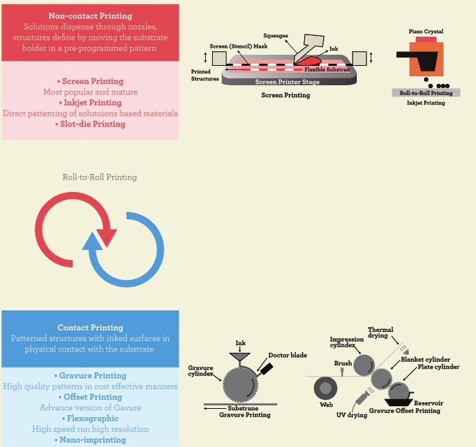
Figure 7: Printing technologies [1]
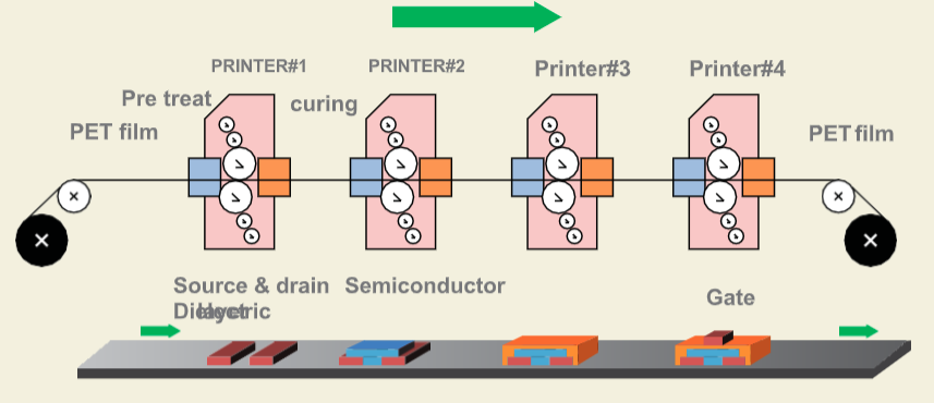
Figure 8: Roll-to-roll printing [1]
Acknowledgements
We greatly appreciate the support of Dr. Unsal KOLDEMIR, Dr. Nazif Uğur KAYA and Mehmet İlker YILMAZ from Kordsa’s R&D Team.
References:
[1] Katsuaki Suganuma, Introduction to Printed Electronics , 2014
[2] Eslamian M. “Inorganic and Organic Solution-Processed Thin Film Devices”. Nano-Micro Letters, 2016
[3] Shah SI, JaGari GH, Yassitepe E, Ali B. “Evaporation”, Handbook of Deposition Technologies for Films and Coatings, Elsevier, 2010
[4] IDTechEx Masterclass, “Introduction to Printed Electronics: Technologies, Players, Markets”, 9-10 April, 2019, Berlin.